
(no title)
ElijahLynn | 17 days ago
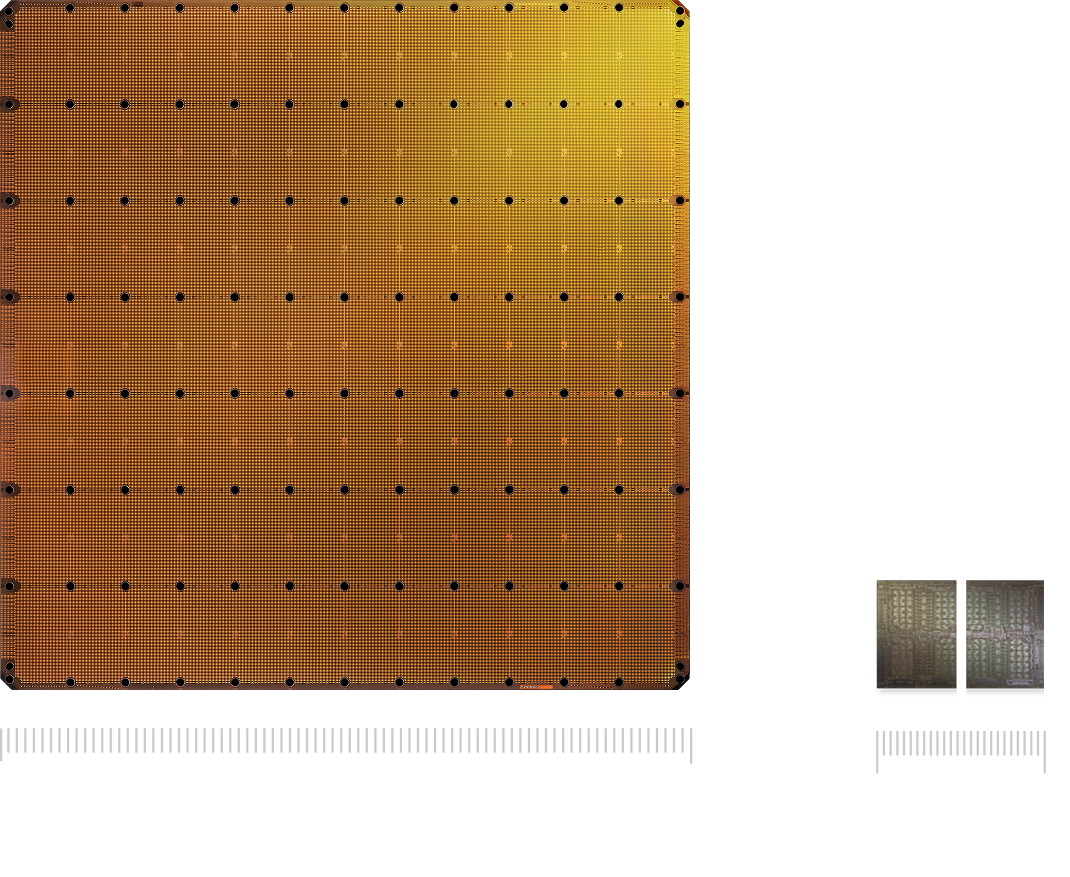
The WSE-3 is the largest AI chip ever built, measuring 46,255 mm² and containing 4 trillion transistors. It delivers 125 petaflops of AI compute through 900,000 AI-optimized cores — 19× more transistors and 28× more compute than the NVIDIA B200.
From https://www.cerebras.ai/chip:
https://cdn.sanity.io/images/e4qjo92p/production/78c94c67be9...
https://cdn.sanity.io/images/e4qjo92p/production/f552d23b565...
dotancohen|17 days ago
ash_091|16 days ago
The correct number is fourty six thousand, two hundred and fifty five square mm.
Sharparam|16 days ago
shwetanshu21|17 days ago
codyb|17 days ago
I was under the impression that often times chip manufacture at the top of the lines failed to be manufactured perfectly to spec and those with say, a core that was a bit under spec or which were missing a core would be down clocked or whatever and sold as the next in line chip.
Is that not a thing anymore? Or would a chip like this maybe be so specialized that you'd use say a generation earners transistor width and thus have more certainty of a successful cast?
Or does a chip this size just naturally ebb around 900,000 cores and that's not always the exact count?
20kwh! Wow! 900,000 cores. 125 teraflops of compute. Very neat
fulafel|17 days ago
graboy|16 days ago
vagrantstreet|16 days ago
"AI" always has some sleazy person behind it for some reason
amelius|16 days ago
carter2099|14 days ago
Pretty cool tech, silicon is very advanced. That said, this is how every wafer comes out of the fab. This process does not dice out individual chips but instead adds interonnects. I doubt they have 100% yield, but probably just don't connect that die. This type of setup is one of the reasons Apple's M series chips are so effective. Their CPU/GPU/RAM are all on one die/directly interconnected instead of going through some motherboard based connector. I think Apple doesn't have them all go through the same process so those are connected via a different process but same layed on silicon direct connection. This solves the problem data centers tend to have of tons of latency for the connections between processors. This is also similar to AMD's infinity fabric of their Zen architecture. It's cool how all of these technologies build from another.
It's also all reliant on fab from TSMC who did the heavy lifting is making the process a reality
elorant|17 days ago
zozbot234|17 days ago
(Bringing liquid cooling to the racks likely has to be one of the biggest challenges with this whole new HPC/AI datacenter infrastructure, so the fact that an aircooled rack can just sit in mostly any ordinary facility is a non-trivial advantage.)
dyauspitr|17 days ago
neya|17 days ago
hugh-avherald|17 days ago
tonyarkles|17 days ago
> Codex-Spark runs on Cerebras’ Wafer Scale Engine 3 (opens in a new window)—a purpose-built AI accelerator for high-speed inference giving Codex a latency-first serving tier. We partnered with Cerebras to add this low-latency path to the same production serving stack as the rest of our fleet, so it works seamlessly across Codex and sets us up to support future models.
https://www.cerebras.ai/chip
thunderbird120|17 days ago
unknown|17 days ago
[deleted]
lanthissa|16 days ago
amelius|16 days ago
Just like potato chips are slices from a potato.
colordrops|16 days ago
DeathArrow|17 days ago
Using a waffer sized chip doesn't sound great from a cost perspective when compared to using many smaller chips for inference. Yield will be much lower and prices higher.
Nevertheless, the actual price might not be very high if Cerebras doesn't apply an Nvidia level tax.
energy123|17 days ago
That's an intentional trade-off in the name of latency. We're going to see a further bifurcation in inference use-cases in the next 12 months. I'm expecting this distinction to become prominent:
(A) Massively parallel (optimize for token/$)
(B) Serial low latency (optimize for token/s).
Users will switch between A and B depending on need.
Examples of (A):
- "Search this 1M line codebase for DRY violations subject to $spec."
An example of (B):
- "Diagnose this one specific bug."
- "Apply this diff".
(B) is used in funnels to unblock (A). (A) is optimized for cost and bandwidth, (B) is optimized for latency.
magicalhippo|17 days ago
Speed will suffer, but it's not like a stuck pixel on an 8k display rendering the whole panel useless (to consumers).
Heathcorp|16 days ago
Basically they use very small cores compared to competitors, so faults only affect small areas.
kumarvvr|17 days ago
zamadatix|17 days ago
santaboom|17 days ago
larodi|17 days ago
txyx303|17 days ago
kreelman|17 days ago
I hope they've got good heat sinks... and I hope they've plugged into renewable energy feeds...
thrance|17 days ago
King-Aaron|17 days ago
xnx|16 days ago
odiroot|16 days ago
tshaddox|16 days ago
https://www.cerebras.ai/blog/100x-defect-tolerance-how-cereb...